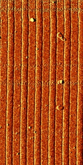
Development of advanced characterization methods by SPM/AFM, S(T)EM or FIB (*). The objective is obtaining information about functional properties at the nanoscale, to support the development of nanoelectronic devices.
(*) SPM/AFM: Scanning Probe Microscopy/Atomic Force Microscopy); S(T)EM: Scanning (Transmission) Electron Microscopy; FIB: Focused Ion Beam.