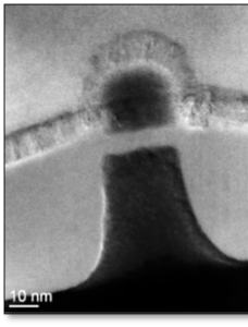
Nanoelectronic devices
The main activities are focused on the development of single-electron transistors (SET) for miniaturized electronic systems with a very low energy consumption, on new topologies for transistor integration and on the development of fabrication technologies for silicon-based spin qubits for quantum computing. The activity includes process and device simulation, including the analysis of variability, and electrical characterization, including at low temperatures.
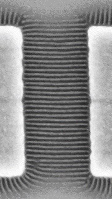
Nanofabrication methods
(i) Top-down techniques: advanced lithographies, e-beam lithography, focused ion beam (FIB)).
(ii) Bottom-up techniques: directed self-assembly of block co-polymers).
(iii) Specific deposition and etching processes.
The aim is to bridge the gap existing between nanofabrication processes for prototyping available in the laboratory and the technology required for applications in pilot lines in the field of micro/nano electronics.
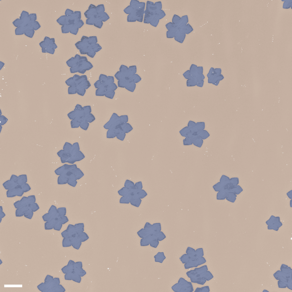
Growth and integration of graphene-based materials for (nano)electronics
This research is dedicated to developing solutions for the large-scale integration of graphene-based materials into (nano)electronic devices and exploring their potential in future integrated circuits and electronic systems. The focus is on the controlled growth of advanced graphene forms — including graphene, graphene nanoribbons (GNRs) and laser-induced graphene (LIG) — as well as on establishing reliable methods for their integration. The goal is to design and evaluate devices and circuit demonstrators to validate their performance and scalability.
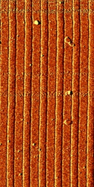
Advanced physical characterization methods
Development of advanced characterization methods by SPM/AFM, S(T)EM or FIB (*). The objective is to have methods available for obtaining information about functional properties at the nanoscale, which is needed for the research performed by the group and for collaborations with other research groups and industries.
(*) SPM/AFM: Scanning Probe Microscopy/Atomic Force Microscopy); S(T)EM: Scanning (Transmission) Electron Microscopy; FIB: Focused Ion Beam.